Soldering and Microsoldering
≈ 7 min read · Print / save as PDF
Soldering is heat + flux + a little solder, for a few seconds. Flux is the secret: if solder will not behave, add flux. Practise on scrap boards until you stop lifting pads.
Solder alloys and temperatures
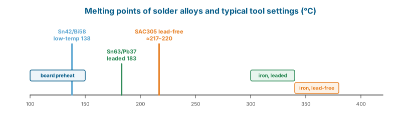
| Alloy | Composition | Melting point | Notes |
|---|---|---|---|
| Sn63/Pb37 (leaded, eutectic) | 63% tin, 37% lead | 183 °C (melts at a single temperature) | Easiest to work with; used by most repair technicians for rework |
| Sn60/Pb40 | 60/40 | 183–190 °C (melting range) | Common wire solder |
| SAC305 (lead-free) | 96.5% tin, 3% silver, 0.5% copper | ≈ 217–220 °C | Used in factory production of nearly all modern electronics (RoHS) |
| Sn42/Bi58 (low-temperature) | 42% tin, 58% bismuth | 138 °C | Used to lower the melting point of factory joints and for separating stacked phone boards; brittle |
Practical consequence: Factory joints are lead-free and melt at about 217 °C. Adding a little leaded solder to a factory joint mixes the alloys and lowers its melting point, making removal easier and gentler on the board. This is standard rework practice.
Typical working temperatures
These are typical starting points; adjust for the tip, the board’s thermal mass, and the station.
| Task | Typical setting |
|---|---|
| Soldering iron, leaded solder, small pads | 300–340 °C |
| Soldering iron, lead-free solder | 340–380 °C |
| Soldering iron on large ground planes / connectors | 360–400 °C with a wider tip |
| Hot air for small passives (0402–0201) | 300–350 °C, low airflow |
| Hot air for QFN chips and connectors | 330–380 °C, medium airflow |
| Hot air for BGA removal (with preheat) | 350–420 °C, depending on board and station |
| Board preheater | 100–150 °C bottom heat |
Hot-air station display temperatures are not standardised between brands — the same “350” can produce different nozzle temperatures. Learn your own station with practice boards and a thermocouple.
Flux
If solder balls up, will not flow, or bridges pins: stop, add flux, and try again. Nine times out of ten, flux fixes it.
Flux removes oxide and lets solder flow. Use plenty of flux on every joint. Without flux, solder balls up, bridges pins, and makes cold joints.
- No-clean flux (gel or paste in a syringe) is the standard for rework. Despite the name, clean residue off with IPA for appearance and to avoid sticky residue.
- Rosin flux is acceptable for general soldering.
- Avoid acid flux (plumbing flux) — it corrodes electronics.
Basic soldering technique (through-hole)
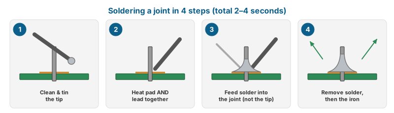
- Clean the tip on brass wool; tin it with a little fresh solder.
- Heat both the pad and the lead together for 1–2 seconds.
- Feed solder into the joint (not onto the iron tip).
- Remove the solder, then the iron. Total contact time ideally under 3–4 seconds.
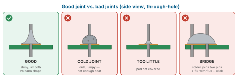
- A good joint is smooth, shiny (leaded) or satin (lead-free), and concave — a “volcano” shape around the lead.
Bad joints:
| Defect | Appearance | Cause |
|---|---|---|
| Cold joint | Dull, grainy, lumpy | Insufficient heat; movement during cooling |
| Dry joint | Solder not wetting the pad | Dirty/oxidised surface, no flux |
| Bridge | Solder connects two pins | Too much solder; fix with flux and wick or a clean tip |
| Lifted pad | Pad peeled off the board | Excessive heat or force |
SMD technique
Removing and fitting small passives (resistors, capacitors)
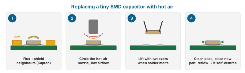
With two irons or tweezers iron: heat both ends simultaneously and lift.
With hot air: apply flux, shield neighbours with Kapton tape if needed, use a small nozzle with low airflow, circle the part until solder melts, lift with tweezers.
Fitting: clean the pads with wick, tin one pad lightly, hold the part with tweezers and reflow that pad, then solder the other pad. Or: apply flux, place the part on tinned pads, and reflow with hot air — surface tension self-centres it.
Desoldering wick (braid)
Place the wick over the joint, add flux, press the iron on the wick. Molten solder wicks into the braid. Do not drag the wick with force on phone boards — it rips pads. Lift straight up while still hot.
QFN and multi-pin ICs
- Flux generously.
- Preheat the board (preheater or broad hot-air sweep).
- Hot air with a nozzle slightly larger than the chip, circling evenly.
- When the solder melts, the chip “floats” slightly — nudge it gently to confirm, then lift.
- Clean pads with wick and flux until flat and evenly tinned.
- Place the new chip with correct pin-1 orientation (dot or bevel marking, matched to the boardview/silkscreen).
- Reflow until it settles; it should self-align.
Connectors (FPC board-to-board, charge ports)
Connectors are plastic and melt. Shield the plastic, use the lowest temperature that works, add low-melt solder to factory joints, and preheat the board from below. On replacement, inspect every pin under the microscope for bridges.
Jumper wires
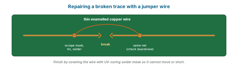
To repair a broken trace or a ripped pad, use fine enamelled copper wire (around 0.01–0.02 mm for phone work; thicker for power lines). Scrape back the solder mask to expose copper at a nearby point on the same net (via the boardview), tin both ends, solder, and secure the wire with UV-curing solder mask. For power rails, use wire thick enough for the current.
BGA rework overview
BGA rework (removing and re-installing chips with solder balls underneath) is advanced and is introduced here only so students understand it:
- Preheat the board; protect nearby components.
- Remove underfill (epoxy) if present — common on phone boards. Underfill must be softened and scraped carefully.
- Lift the chip with hot air or a rework station once all balls melt.
- Clean the board pads and chip pads flat with wick.
- Reball the chip using a stencil, solder paste or solder balls of the correct size, and hot air.
- Flux the board, align the chip, reflow.
Typical BGA work in shops: replacing a laptop GPU, swapping a phone’s NAND or a charging IC, and reballing. Success requires practice on scrap boards.
Note on “reflowing”: Heating a BGA chip without removing it to “fix” a failing GPU solder joint (the old “oven trick” or hot-air reflow) is at best a temporary measure. The underlying failure — cracked solder balls or a failing chip — usually returns. Do not sell a reflow as a permanent repair; replace the chip or offer an honest short warranty.
Stacked (“sandwich”) phone boards
Since the iPhone X, many iPhones (and some Android phones) use a two-layer stacked logic board: an upper board (SoC side) and a lower board (often RF/modem side) joined by an interposer. Separating them is required for some repairs (e.g. reaching components between the layers). It uses a board preheater or dedicated separation fixture, often with low-temperature solder, and careful prying. It is an advanced skill; practise only on scrap boards.
Watch and read
- Watch: Soldering basics — YouTube search: how to solder for beginners
- Watch: Hot-air SMD replacement — YouTube search: hot air rework SMD capacitor replacement tutorial
- Watch: Getting started with microsoldering — YouTube search: microsoldering for beginners practice board
- Watch: Jumper wires on broken traces — YouTube search: jumper wire repair trace microsoldering
- Read/use: SparkFun — How to Solder (through-hole) — Tools, technique and rework, with photos.
- Read/use: Adafruit Guide to Excellent Soldering — Classic illustrated guide: good and bad joints.
Review questions
- Why does adding leaded solder to a factory joint make rework easier?
- Give the melting points of Sn63/Pb37, SAC305 and Sn42/Bi58.
- Why must flux be used on every joint?
- Describe the procedure to replace a 0402 capacitor with hot air.
- Why is BGA “reflow” not a reliable permanent repair?
Lab exercises
Lab 4.1 — Through-hole. Solder 30 through-hole joints on a practice kit; instructor grades each joint.
Lab 4.2 — SMD passives. Remove and replace twenty 0805, twenty 0603 and twenty 0402 components on a practice board. Target: no lifted pads, no bridges.
Lab 4.3 — QFN. Remove and refit a QFN regulator on a scrap laptop board; confirm with diode mode afterwards.
Lab 4.4 — Jumper wire. Cut a trace on a scrap board and repair it with a jumper wire secured with UV mask. Confirm continuity.
Lab 4.5 — Connector. Replace a board-to-board FPC connector on a scrap phone board without melting the plastic housing.